Graphene innovation in Finland is leading the way in emerging applications
Graphene innovation in Finland is leading the way in emerging applications
In Finland, PhD graduates are welcomed to wear a ceremonial top hat and sword for their graduation. This unusual tradition is just one of the country’s curious quirks. For instance, did you know there are more saunas than cars in Finland?
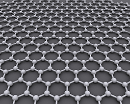
What’s also lesser known is Finland’s extensive contribution to graphene research through European project, the Graphene Flagship. Starting from the joint interest of Nokia and Finnish research institutes, soon after the experimental discovery of graphene and related materials (GRM) in 2004, VTT Technical Research Centre of Finland (VTT) began developing its research in this area and now plays a vital role in the Graphene Flagship.
VTT provides a shining example of incredible scientific research currently occurring in the Nordics. Headquartered in Espoo, Finland, VTT describes its research centre as a ‘sweet spot for innovation’ with a vision to change companies and wider society through new science-based innovations.
VTT’s interest in graphene sparked from discovering the potential of this new 2D material in sensing applications and has always had a strong focus on scalable production methods; after attempting to produce wafer-scale monolayer graphene by transfer printing from layered graphite, they established in-house chemical vapour disposition (CVD) in 2010 and began to work with printed GRMs.
Since then, the centre’s interest in graphene has blossomed and paved new opportunities to explore other potential application fields for 2D materials, especially those where VTT already has strong levels of expertise. One of the most important application areas for graphene at VTT is biosensors – devices that measure biological or chemical reactions by quantifying an electrical response.
Why use graphene for electrical quantitative biosensors?
Graphene has several advantages to enable the emergence of point of care (POC) and point of application (POA) electrical quantitative biosensors, both for the professional use in the healthcare and food industries, and for home appliances such as medication feedback and health hacking. The chemical stability and high sensitivity of graphene, together with the easy integration with CMOS – complementary metal-oxide semiconductor – readout to enable statistics and biological multiplexing, can dramatically improve both the cost structure and the accuracy of the data collected by the biosensors.
VTT has recently demonstrated CMOS integrated graphene FET biosensor matrices and aims to develop the concept to be applied with their biosensor cloud interface in order to demonstrate its compatibility with home diagnostics. In this area, VTT combines its expertise on material science, IC design, protein- and antibody engineering and biosensor system integration.
The other strong application areas of VTT where CVD graphene and 2D semiconductors are applied are in THz and infrared detectors, hyperspectral imaging, integrated photonics and quantum technologies. VTT also provides graphene integration services for companies and universities in Europe and globally, from initial device and product development to small- and medium-scale production.
The substrate independence of 2D materials have also piqued the interest of VTT researchers working in the field of flexible electronics. The combination of high conductivity graphene with excellent RF performance and 2D semiconductors allowing logic operations, pave the way for large area sensor multiplexing and future wireless communications on flexible platforms, including body area network (BAN), and at the other end, neuromorphic computing.
Latest graphene applications
Considering these emerging applications, many of the devices need thin film transistors that are distributed over large areas. The commonly used silicon-based IC chips need to be integrated as separate elements, which is not always the best option, and flexible 3D semiconductors require relatively high temperature processes. Here VTT aims to develop heterogeneous solutions based on large area 2D materials, carbon nanotubes and printed metal-oxide materials.
VTT can collaborate with commercial clients from the material development process to production scale-up and system integration, making graphene-enabled flexible electronics a potentially fruitful area for manufacturers in the electronics space.