


Designing a successful wireless product with an antenna requires some additional steps in the design cycle. An antenna cannot be simply ‘added’ at the end like a shield can or some copper tape, the RF aspect of the design needs to be a priority from the outset. Here Geoff Schulteis, Senior Antenna Applications Engineer with Antenova takes us through seven steps to an optimised design that will perform well, without unexpected performance drops and failed certification efforts.
1. Antenna selection
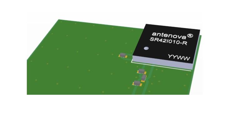
There are several antenna groups to choose from. Surface-mount devices (SMD), also called surface mount technology (SMT) antennas are the most popular antennas available today. They are tiny and mount directly to the PCB, and are available in high-grade dielectric laminate substrates, ceramic and even stamp metal.
Similarly, there are antenna modules. These offer the advantage of coming pre-assembled with the antenna chip and other key components in a readymade solution. They can effectively be dropped into a design without spending too much time on designing RF circuitry.
For applications which use non-RF friendly materials – such as metal – near the antenna, it will prove difficult to achieve strong wireless performance levels with an embedded antenna, but a case-mounted (or Terminal) antenna, which has a layer of material for isolation, can perform with minimal losses. Case-mounted antennas are less sensitive to other components nearby, so they are easier to design in than SMD antennas, and they free up space on the PCA for other components.
Flexible printed circuits, or FPC antennas also save space, and are popular for devices with limited PCA length. They can be wrapped around the housing of a device and connected onto the circuit board by a small surface mount connector.
2. Antenna placement
The antenna may be the only component that needs to be placed in a specific physical position, so it is logical to place it first.
It is important to understand how the placement of the antenna will affect its performance, particularly with an SMD antenna. The antenna should be positioned away from the rest of the RF and digital circuitry because noise from other components can degrade the received signal and impedance performance.
Most antennas perform best on the corner of the PCB. However, some antennas operate best along the longest edge. The manufacturer’s data sheet and evaluation board will guide you to the best position for an individual antenna.
Consider too, how close the antenna will be to the casing for the device. Plastic has a higher dielectric constant than air, so placing an antenna too close to it is likely to detune the antennas resonant frequency bands and limit the antenna performance.
3. Board design
Antennas use ground planes in order to radiate efficiently, so allowing the correct length for the ground plane will help the antenna to perform correctly. The manufacturer’s datasheet and evaluation board will show the recommended ground plane length for the chosen antenna.
Antennas have unique keep-out requirements which should be free of any components. We recommend placing noisy and metallic components such as batteries and motors away from antennas, where possible.
Position the radio module as close as possible to the antenna to reduce the length of the antenna’s feed trace. Longer transmission lines are more prone to reflections and signal losses which can reduce antenna performance.
4. Gerber design review
At this stage, the designer should check that the board layout is optimised for RF performance. If the device uses a transmission line, it should match the source impedance and RF circuitry, and it will be best if the lines are short, without sharp bends.
Some designs will benefit from a matching circuit (such as a Pi matching circuit) within the RF circuitry to tune the antenna for improved performance.
5. Design test
It is critical to test the design, to be sure that the finished device will perform correctly.
All cellular operators test the devices that are to operate on their networks, these tests are particularly tough in North America, so conducting radiated performance testing early on in the design cycle helps to get a successful outcome, and gain network certification for the design without delays.
Testing in an anechoic chamber shows how the antenna performs on its PCB, then the next stage, over-the-air testing shows how the antenna performs when it has been integrated into the device. The results will be measured as return loss and passive antenna efficiency, active Total Radiated Power & Total Isotropic Sensitivity, and radiated spurious emissions.
6. Pre-production checks
We recommend checking that the material used for the PCB in production matches that used for the prototype, as altering the material can alter RF performance. Reflow soldering processes during manufacture can expose components to high temperatures, check these will not be hotter than the temperatures rated for the antenna.
7. Mass production
When the design reaches production, assembly times, component costs and production scalability will become key concerns. Designs using SMD antennas can be assembled by pick-and-place machinery, but products with FPC and case-mounted antennas will need to be assembled by hand. SMD antennas are therefore more cost-effective in manufacture.