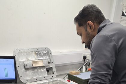

How smarter sensors can overcome barriers to additive manufacturing adoption
Ross Turnbull, director of product engineering and business development at Swindon Silicon Systems, shares how smarter sensors can overcome barriers to additive manufacturing adoption
Analysis by additive manufacturing (AM) consultancy group, Wohlers, shows that in 2024 the global AM industry grew to $21.8 billion. Despite this growth, the report indicates that 2024 was a year of mixed performance, suggesting barriers still prevent mass uptake. Mixed-signal ASIC design company Swindon Silicon Systems is addressing these hurdles through the development of smarter sensors.
As industrial demands evolve, customers are increasingly seeking solutions tailored to specific performance and functional requirements. AM technologies help meet these needs.
Thanks to its layer-by-layer assembly process, AM can create highly complex shapes and geometries in a single step. This capability accelerates the journey from digital concept to physical prototype and eliminates the need for specialised moulds or tooling. Furthermore, when parts must fit precisely within tight spaces or alongside other components, AM enables early verification of fit and function without the expense of full-scale manufacturing.
AM technologies also enable manufacturers to be more flexible and tailor products to specific needs, supporting differentiation and stronger customer-manufacturer relationships. However, challenges still remain in successfully implementing and using this technology.
UNDERSTANDING THE OBSTACLES
Research conducted by the World Economic Forum highlights that 53% of companies surveyed saw quality assurance and qualification as the primary barrier to adopting AM.
Poor layer adhesion, cracks and warping are common problems. In large-scale production, especially in aerospace and automotive sectors, even minor discrepancies in product quality can have serious consequences. Such defects often lead to elevated costs, production delays and costly recalls that could damage a manufacturer’s reputation.
Due to this risk, manufacturers need better visibility over their processes. Tracking process parameters allows defects to be detected and corrected before compromising a component’s structural integrity or performance. Optical sensors are well-suited to AM, providing detailed insight into surface characteristics and internal features. Technologies like monochrome or colour CCD and CMOS sensors can detect surface flaws and irregularities during production. While this technology has come a long way, it still faces limitations in AM processes.
In these environments, sensors must produce clear, low-noise data for accurate signal interpretation and informed decision-making. So, how can we ensure this?
ENHANCING SENSOR PERFORMANCE
To answer that, we need to examine the sensors’ components more closely. In most sensors, the sensing element is typically combined with one or more integrated circuits (ICs) that serve as the interface. These ICs handle signal conversion, processing tasks and translate light intensities into electronic signals that can then be interpreted and acted on by other devices.
However, standard ICs can struggle with precise signal processing, resulting in unreliable data. This is a serious drawback in advanced AM processes when accurate feedback is critical for closed-loop control and automation. In addition, inconsistent performance and limited reliability make it difficult to meet the rigorous quality assurance and qualification standards expected in industrial environments.
A more effective approach is to use a custom-built solution tailored to the application. An Application Specific IC (ASIC) is a bespoke chip that can be designed to meet precise performance and environmental requirements, including overcoming the aforementioned challenges.
In AM, quick, precise adjustments are essential during production to ensure layer consistency, maintain dimensional accuracy and prevent defects that compromise part quality. An ASICs design allows for optimised on-chip processing, supporting these adjustments without relying on external systems. This makes them especially valuable in closed-loop control systems, where real-time feedback is critical for maintaining quality and process stability.
ASICs can also be fine-tuned with sensor-specific protocols to deliver superior image clarity and resolution. This level of customisation enables the sensor to identify even the smallest inconsistencies in a build layer, such as porosity, warping or minor structural anomalies that can compromise the integrity of a component. By providing this targeted performance, ASICs ensure more reliable data acquisition and significantly reduce the risk of quality issues in AM production.
Full control over the ASIC’s design also means the component has a smaller footprint than other solutions, making the sensor easier to integrate into existing machinery. With a customisable choice of wired and wireless communication protocols available, ASICs can support both new and legacy equipment.
Additive manufacturing has the potential to transform large-scale production by enabling complex components to be machined from a wide range of materials in a single step. However, sensing systems must be enhanced for this technology to be widely adopted. Here, ASICs offer a key advantage, providing tailored solutions to address specific AM process sensor needs.